
Final month Samsung Foundry quietly introduced that it was set to start producing chips utilizing its 3GAE (3 nm-class, gate-all-around transistors, early) course of know-how within the second quarter. Whereas the business’s first 3 nm-class node with GAA transistors is a noteworthy achievement by itself, one factor that’s significantly necessary is that to make GAA transistors effectively, fabs need to be outfitted with new manufacturing instruments. Fittingly, Utilized Supplies has not too long ago outlined their subsequent era of instruments that will probably be used to allow Samsung (and different fabs) to construct their first GAA chips.
Gate-All-Round Transistors: Fixing Many Issues at As soon as
New course of applied sciences ought to allow greater efficiency, decrease energy, and better transistor density to satisfy necessities of chip designers. However this mix has been significantly arduous to attain within the current years as shrinking transistor sizes result in adverse results like leakage present. To maintain scaling efficiency and voltages whereas minimizing transistor sizes, the business started transition from planar to FinFET transistors (which elevated the contact space between the channel of the transistor and the gate by making the gate taller) in 2012 and the sort of transistors will stick with us for a very long time. However the tempo of FinFET-based nodes innovation is slowing down as adverse elements of transistors shrinking beginning to kick in.
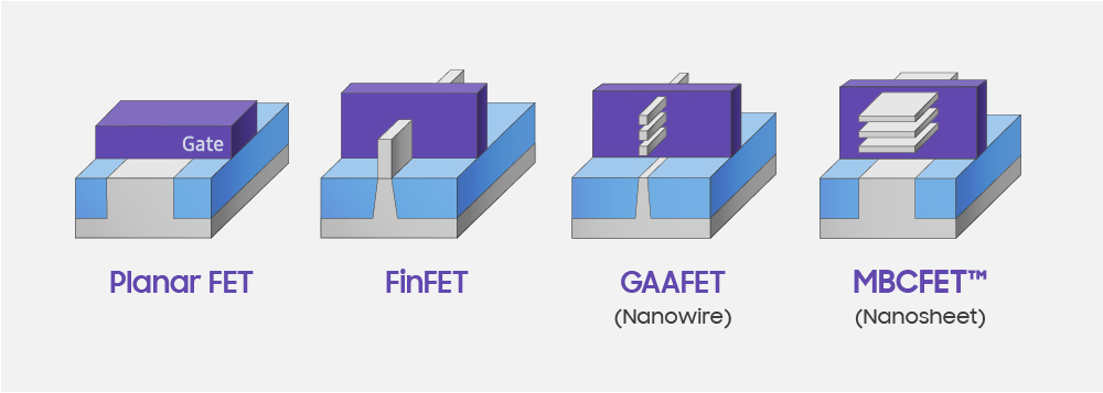
Ever since Intel launched its 22 nm FinFET-based know-how over a decade in the past, chipmakers started to speak in regards to the subsequent inevitable step in transistor design, which is gate-all-around. Because the title suggests, in GAAFETs channels are horizontal and are surrounded by gates round all 4 sides of the channels, which solves many issues related to the leakage present. However this isn’t the one benefit: in nanosheet/nanoribbon-based GAAFETs it’s attainable to regulate channel width to get greater efficiency or scale back energy consumption. Since Samsung’s 3GAE and 3GAP applied sciences use nanosheets, Samsung calls its GAAFETs multi-bridge channel field-effect transistors (MBCFETs) to emphasise that it doesn’t use nanowires. Moreover, Utilized Supplies claims that GAA structure reduces transistor variability, which implies improved yields and quicker time-to-yield (at the least so far as transistor efficiency is anxious) and reduces cell space by 20% to 30%.

Whereas all chipmakers have been speaking about GAAFETs and their benefits over FinFETs at numerous academia business occasions, Samsung was the primary firm to announce a transition to the brand new sort of transistors with its 4 nm node generally in 2022 ~ 2023. Ultimately, the corporate’s plans modified a bit and in 2019 it unveiled its GAAFET-based 3GAE and 3GAP nodes with excessive quantity manufacturing due in 2022 and 2023, respectively. Final 12 months the corporate re-emphasized plans to kick off manufacturing utilizing its 3GAE in 2022 and this quarter it mentioned that quantity manufacturing was set to begin in Q2.
However Manufacturing Is Difficult
However manufacturing of chips utilizing any modern course of know-how is difficult and making merchandise utilizing Samsung’s MBCFET-based 3GAE node definitely poses some dangers not solely as a result of we’re speaking a few 3 nm-class manufacturing course of, however as a result of manufacturing of GAA transistors is totally different than making FinFETs.
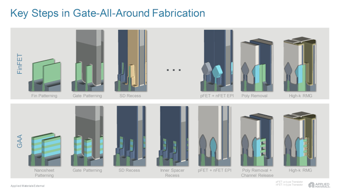
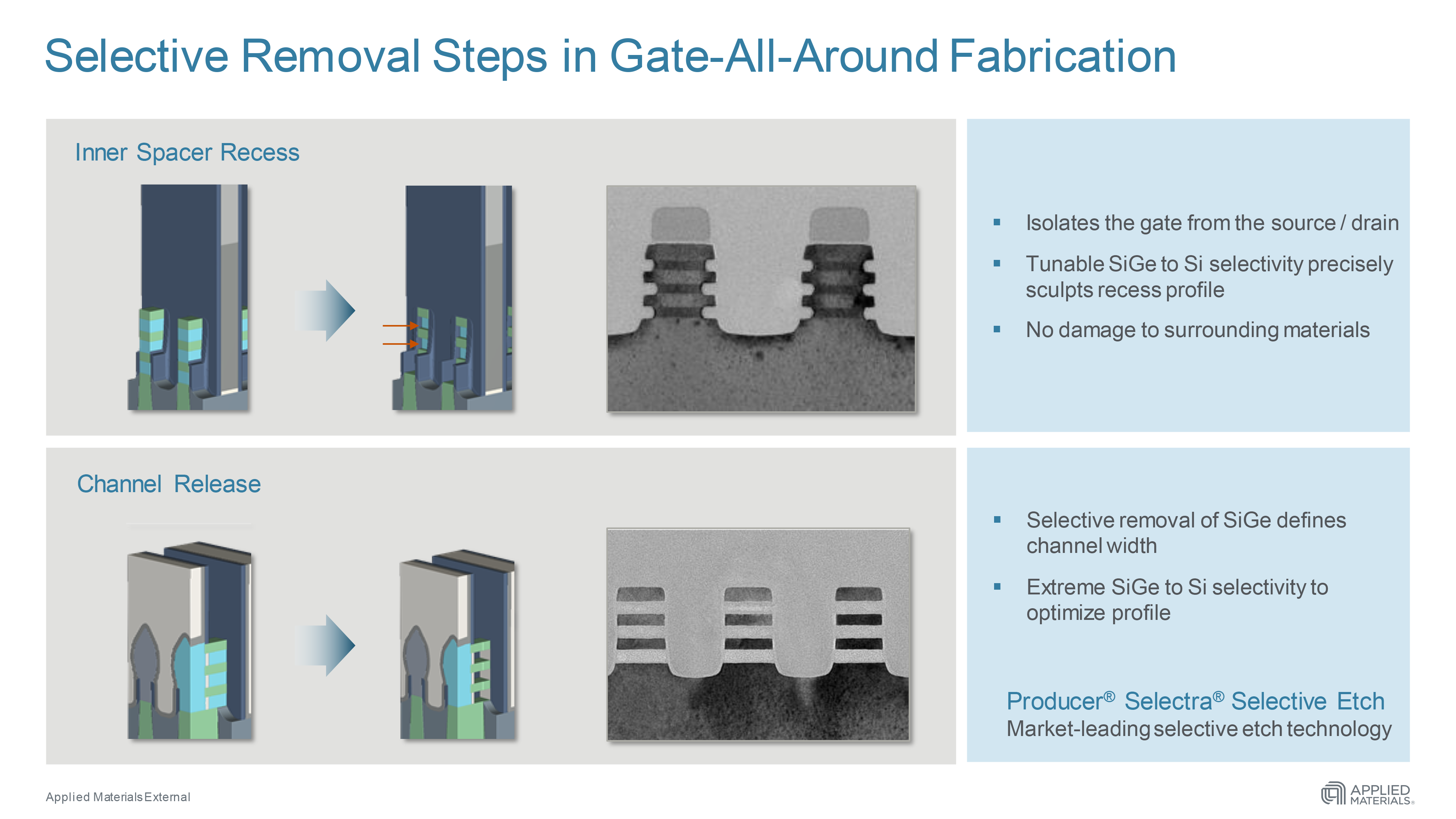
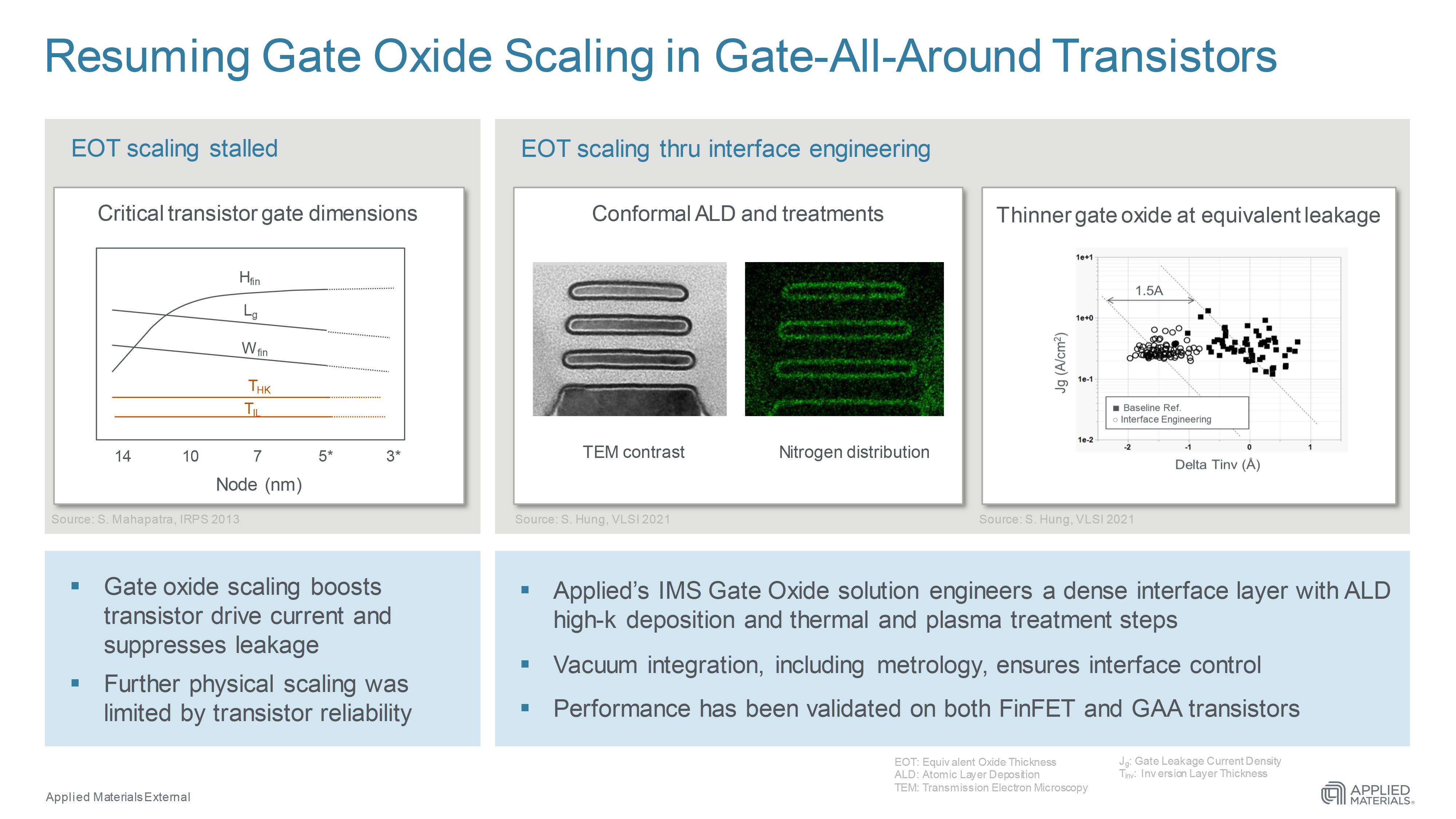
Channels of GAA transistors are formed utilizing lithography, epitaxy and selective supplies removing, processes that allow chipmakers to fine-tune width and uniformity for optimum energy and efficiency. These epitaxial steps are significantly extra complicated when in comparison with these with FinFETs as producers must deposit the multi-layer gate oxide and metallic gate stacks across the tiny 10 nm channels, which is a key problem with GAAFETs. That is the place Utilized’s high-vacuum Built-in Supplies Answer (IMS) programs come into play.
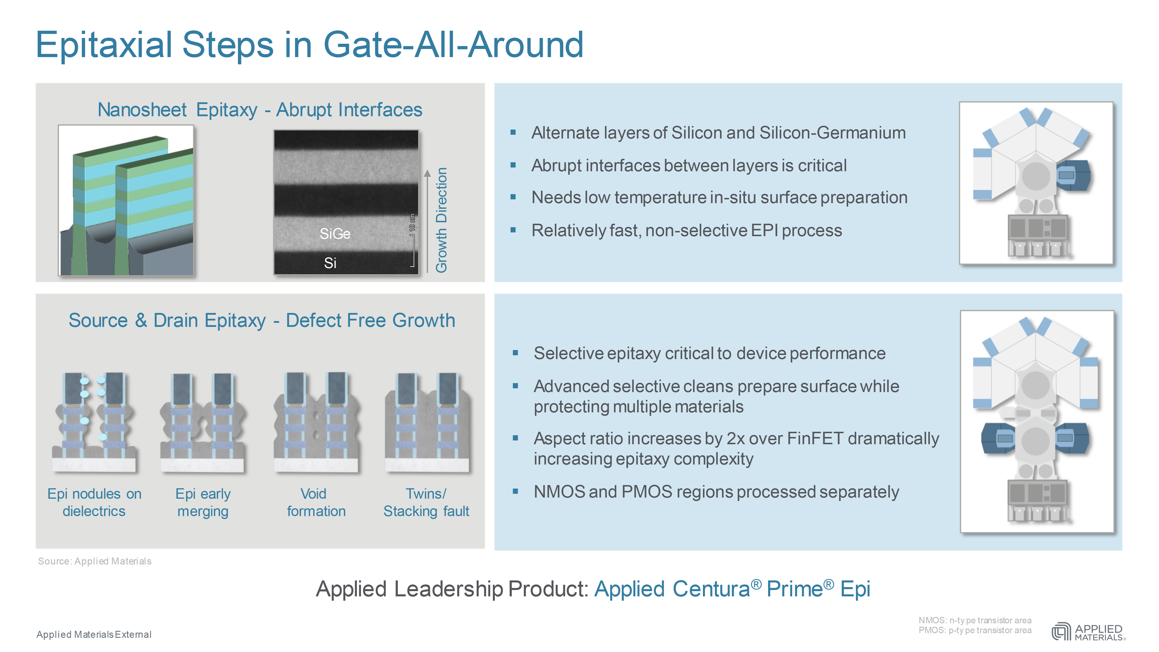
Firstly, Utilized’s Producer Selectra Selective Etch IMS device removes pointless SiGe to isolate the gate from the supply/drain and outline channel width with out damaging surrounding supplies. Secondly, the Utilized Centura Prime Epi IMS device can deposit an ultra-thin gate oxide layer utilizing built-in atomic layer deposition (ALD), thermal, plasma therapy, and metrology steps. Utilized’s IMS can scale back gate oxide thickness by 1.5 angstroms in comparison with competing resolution, which permits to make gates thicker and allow greater drive present and due to this fact transistor efficiency with out growing present leakage, which is a consequence of skinny gates.
Utilized launched its first Selectra etching system in 2016 and since then has shipped over 1,000 chambers which might be presently in use by its prospects, so the business is kind of conscious the best way to use them. Whereas etching is a extensively used course of, its utilization and significance will develop because the business begins to transit to newer course of applied sciences, together with these primarily based on GAA transistors.
It’s essential to notice that numbers shared by Utilized Supplies come from numerous corporations (together with TSMC and Qualcomm) and shouldn’t be utilized solely to Samsung Foundry’s 3GAE and 3GAP nodes. In the meantime, the overall benefits of GAA/MBC/nanoribbon/nanosheet transistors, in addition to challenges with their manufacturing, are related for the entire business.
Samsung’s 3GAE: +30% Efficiency, -45% Space
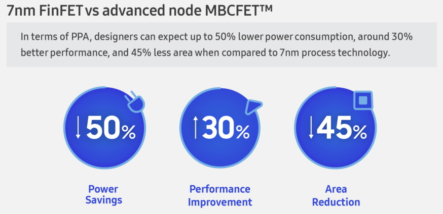
Talking of benefits, Samsung expects its 3GAE course of to supply a 30% efficiency improve or a 50% energy consumption discount, and a forty five% space discount when in comparison with 7LPP. Such tangible advantages could also be sufficient to justify challenges related to this transition within the brief time period.
For now, the use of 3GAE manufacturing know-how that depends a brand-new transistor construction is difficult usually, as in addition to new digital design automation (EDA) instruments, Samsung might want to invent new IP, and undertake brand-new design guidelines. All of this stuff, when mixed with new lithography, new etching, and new deposit steps are going to make Samsung’s transition tough.
However in change, it can begin gaining expertise with GAA transistors years forward of Intel and TSMC, which can carry sure positive factors within the long-term future. Moreover, expertise with GAAFETs will probably be helpful for Samsung’s DRAM manufacturing as reminiscence significantly advantages from smaller cell sizes and better transistor densities.
