TSMC this afternoon has disclosed that it’s going to broaden its manufacturing capability for mature and specialised nodes by about 50% by 2025. The plan consists of constructing quite a few new fabs in Taiwan, Japan, and China. The transfer will additional intensify competitors between TSMC and such contract makers of chips as GlobalFoundries, UMC, and SMIC.
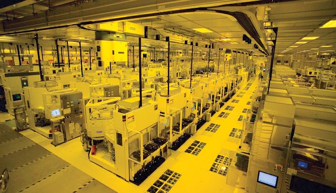
Once we speak about silicon lithography right here at AnandTech, we principally cowl modern nodes used produce superior CPUs, GPUs, and cell SoCs, as these are units that drive progress ahead. However there are a whole lot of system varieties which can be made on mature or specialised course of applied sciences which can be used alongside these refined processors, or energy rising sensible units which have a major impression on our day by day lives and have gained significance within the current years. The demand for numerous computing and sensible units within the current years has exploded by a lot that this has provoked a world chip provide disaster, which in flip has impacted automotive, client electronics, PC, and quite a few adjoining industries.
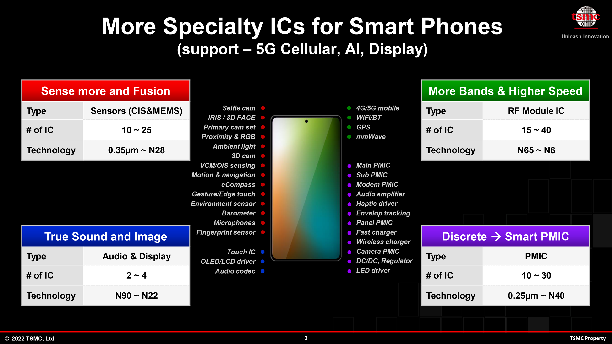
Trendy smartphones, sensible dwelling home equipment, and PCs already use dozens of chips and sensors, and the quantity (and complexity) of those chips is barely rising. These elements use extra superior specialty nodes, which is likely one of the purpose why firms like TSMC should broaden their manufacturing capacities of in any other case “outdated” nodes to satisfy rising demand within the coming years.
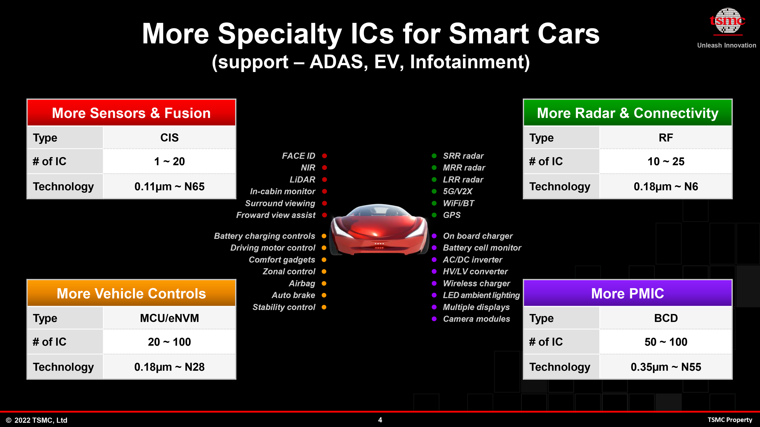
However there’s one other market that’s about to blow up: sensible automobiles. Automobiles already use a whole lot of chips, and semiconductor content material is rising for autos. There are estimates that a number of years down the highway the variety of chips per automotive will likely be about 1,500 models – and somebody should make them. Which is why TSMC rivals GlobalFoundries and SMIC have been rising investments in new capacities within the final couple of years.
TSMC, which has among the many largest CapEx budgets within the semiconductor industries (which is challenged solely by Samsung) has lately been comparatively quiet about their mature and specialty node manufacturing plans. However at their 2022 TSMC Expertise Symposium, the corporate outlined its plans formally.
The corporate is investing in 4 new services for mature and specialty nodes:
- Fab 23 Part 1 in Kumamoto, Japan. This semiconductor fabrication facility will make chips utilizing TSMC’s N12, N16, N22, and N28 nodes and could have a manufacturing capability of as much as 45,000 300-mm wafer begins per thirty days.
- Fab 14 Part 8 in Tainan, Taiwan.
- Fab 22 Part 2 in Kaohsiung, Taiwan.
- Fab 16 Part 1B in Nanjing, China. TSMC presently makes chips on its N28 in China, although the brand new section was as soon as rumored to be able to making chips utilizing extra superior nodes.
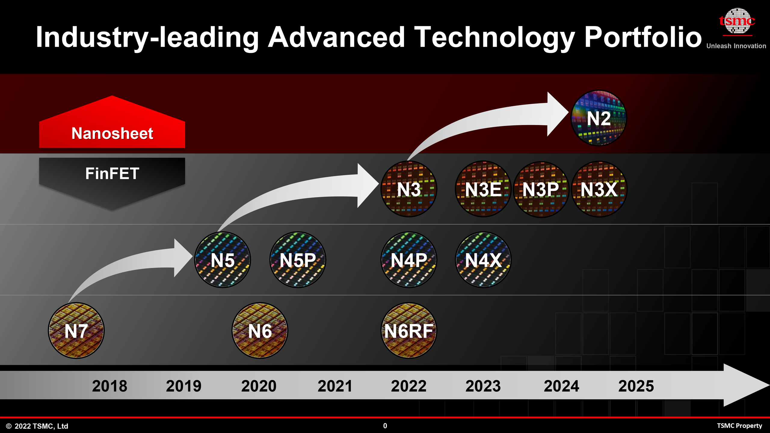
Rising mature/specialised capability by 50% over the subsequent three years is a giant shift for the corporate, and one that may enhance TSMC’s aggressive positions in the marketplace. What is probably extra essential is that the corporate’s specialty nodes are largely based mostly on its frequent nodes, which permits a minimum of some firms to re-use IP they as soon as developed for compute or RF for a brand new utility.
“[Our] specialty expertise is kind of distinctive as it’s based mostly on frequent expertise platform [logic technology platform], so our distinctive technique is to permit our buyer to share or reuse most of the [common] IP,” mentioned Kevin Zhang, senior vice chairman of enterprise growth at TSMC. “For instance, you’ve got RF functionality, you construct that RF on a typical logic platform, however later you discover ‘hey somebody want a so-called ULV function to help an IoT product utility.’ You need to construct that on a typical platform so you possibly can enable completely different product strains to have the ability to share IP throughout the board, this is essential for our clients so we do need to present a built-in platform to handle the market wants of buyer from product perspective.’
There are different benefits too. For instance, TSMC’s N6RF permits chip designers to mix high-performance logic with RF, which allows them to construct merchandise similar to modems and different, extra distinctive options. Many firms are already accustomed to TSMC’s N6 logic node, so now they’ve a chance so as to add RF connectivity to one thing that advantages from excessive efficiency. GlobalFoundries has an analogous method, however because the U.S.-based foundry doesn’t have something corresponding to TSMC’s N6, TSMC has an indeniable benefit right here.
With its frequent platform method for mature nodes in addition to specialised applied sciences, and 50% extra capability, TSMC will be capable of provide the world extra chips for sensible and related units within the coming years. Moreover, it can additionally profit TSMC by considerably rising the corporate’s revenues from mature and specialised nodes, in addition to rising stress on their rivals.
