
TSMC’s FinFlex Know-how Allows Higher Design Flexibilty

In line with TSMC, FinFlex provides it higher design flexibility and makes it simpler for chip designers to positive tune efficiency and energy consumption, balanced with value, all whereas maximizing transistor density. That is particularly vital because the market as an entire embraces hybrid CPU designs.
“The TSMC FinFlex innovation provides decisions of various normal cells with a 3-2 fin configuration for extremely efficiency, a 2-1 fin configuration for finest energy effectivity and transistor density, and a 2-2 fin configuration offering a steadiness between the 2 for Environment friendly Efficiency,” TSMC explains.

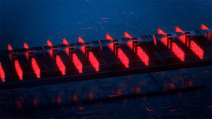
Proven within the picture above is an instance of an N3 structure the place the chip designer can select the perfect Fin configuration for every practical block on a chip. A 3-2 Fin allows the quickest clock frequencies and finest efficiency; a 2-2 Fin association provides a steadiness between efficiency, energy effectivity, and density; and a 2-1 Fin allows the bottom energy consumption with the bottom leakage and highest density of the bunch.
Notice that FinFlex doesn’t substitute personalized nodes and specialised libraries, but it surely’s one other approach that chip designers can tune their designs primarily based on their energy, efficiency, and price targets.
TSMC Appears to be like Forward To 2 Nanometers (2N) In 2025

The opposite technological introduction with N2 is a bottom energy rail. This goes hand-in-hand with GAAFETs to enhance the performance-per-watt proposition.

TSMC claims its N2 know-how will ship a 10-15 % pace enchancment on the identical energy versus N3E, or a 25-30 % energy discount on the identical pace. This, based on TSMC, will usher in a brand new period of environment friendly efficiency.
“N2 will function nanosheet transistor structure to ship a full-node enchancment in efficiency and energy effectivity to allow next-generation product improvements from TSMC prospects. The N2 know-how platform features a high-performance variant along with the cellular compute baseline model, in addition to complete chiplet integration options,” TSMC says.
Apparently, the advance in transistor density will within the neighborhood of 10 % versus N3E. That is not earth shattering, and N3S might shut the hole, albeit on a distinct course of know-how. That would set the state for some fascinating chip design choices down the road.
