Intel introduced the primary particulars of its ‘Intel 4’ course of node and shared a picture of a Meteor Lake compute die on the 2022 IEEE VLSI Symposium. Intel claims spectacular outcomes with its new ‘Intel 4’ node over its previous-gen ‘Intel 7’ node, together with 21.5% increased frequencies on the identical energy, or a 40% energy discount on the identical frequency. Intel additionally claims a 2X space scaling enchancment, which means it has doubled transistor density for the high-performance libraries. The Intel 4 node can also be the corporate’s first to make use of EUV lithography. That is simply to call a couple of amongst many different notable developments that we’ll cowl in additional element under.
Intel’s missteps with the 10nm course of noticed it lose its course of tech management to TSMC, to not point out cede efficiency management to AMD within the CPU market. As such, all eyes are on the corporate as its ‘Intel 4’ course of, which we’ll confer with as ‘I4,’ involves market in 2023.
Final time, Intel tried to scale too aggressively with its 10nm node and attain a 2.7X scaling aim. That led to fixed delays because of the incorporation of a number of new applied sciences concurrently, a few of which clearly did not meet growth targets. For I4, intel is taking a extra modular strategy and introducing newer applied sciences step-by-step because it progresses from node to node, thus serving to it obtain a extra gradual cadence that it hopes will keep away from the delays we have seen up to now.
Intel is growing a number of nodes in parallel to ship on its promise of 5 nodes in 4 years, and Intel 4 is the second step in that journey. First, let’s take a more in-depth take a look at the Meteor Lake die, then dive into the small print of the I4 presentation.
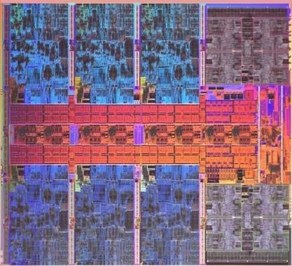
Intel Meteor Lake Die Shot
Intel’s Meteor Lake would be the first product to market with the I4 course of. Intel powered on the compute silicon in April 2022 and claims it has already booted a number of working techniques. Intel says Meteor Lake is on observe for a 2023 launch.
Meteor Lake will use Intel’s Foveros 3D packaging tech, simply as we noticed with the Lakefield processors. Nevertheless, this can be Intel’s first foray into high-volume manufacturing with this modern packaging tech.
Intel will join the 4 die (referred to as ’tiles’ in Intel parlance) to an interposer by TSV connections. Intel hasn’t disclosed if this interposer can be lively or passive or if it should maintain caches or different management circuitry. Intel will mount 4 tiles atop this interposer: the compute tile, I/O tile, SOC tile, and graphics tile.
Intel has specified that compute tile will use I4 however hasn’t mentioned which nodes it should use for the opposite tiles. Throughout its Analyst Day earlier this 12 months, the corporate shared the slide within the above album that lists TSMC’s N3 (3nm) node with the Meteor and Arrow Lake processors. That is largely thought to comprise the graphics tile. Time will inform.
As with Alder Lake, the Meteor Lake chips have an x86 hybrid structure. On this case, we now have six p-cores and eight e-cores. The exploded view of the compute die exhibits us six blue-colored Redwood Cove efficiency cores (p-cores), used for latency- and performance-sensitive work, on the left of the die. To the best, we see two four-core clusters of Crestmont effectivity cores (e-cores) in purple. These cores step in for background and multi-threaded duties. The middle of the chip incorporates the L3 caches and interconnect circuitry. Intel has but to supply an additional description of the variations between the SoC and I/O tiles, with the previous a probable candidate for reminiscence controllers and PCIe interfaces, whereas the latter might be for Thunderbolt and different PCH-types of interfaces.
Intel is not giving us a lot to work with right here, however the firm shared much more expansive particulars on the I4 course of node that makes the compute die tick.
Intel 4 Course of Node
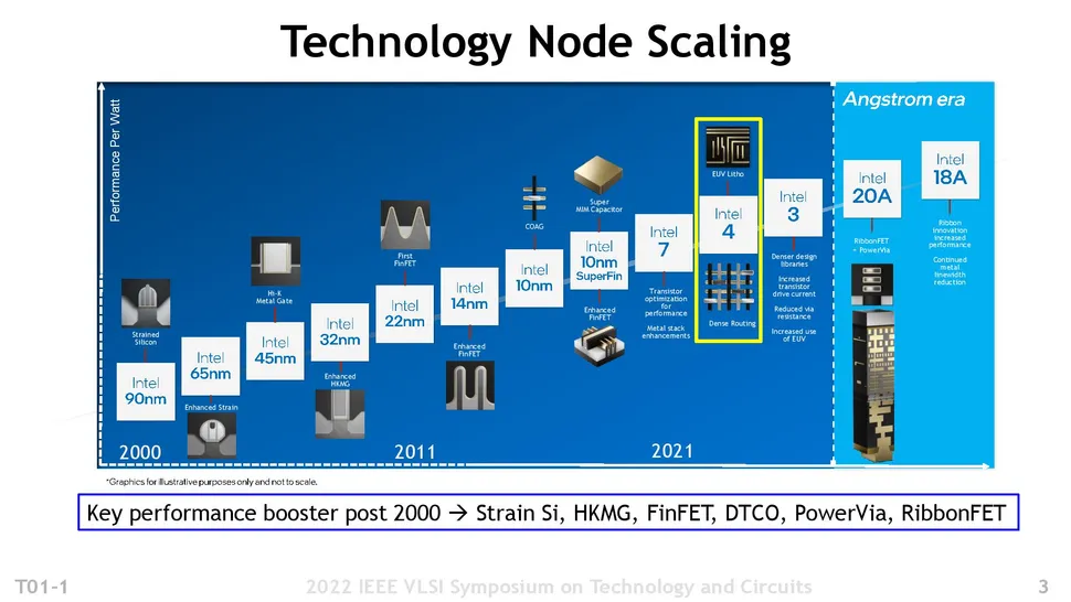
As a fast reminder, Intel not too long ago renamed its course of nodes to have a extra uniform naming conference that aligns with its major rivals (third-party foundries TSMC and Samsung). Intel’s present flagship course of node, Intel 7, was once referred to as 10nm. Moreover, the I4 node was once known as 7nm. We’ll persist with the present naming scheme so there isn’t any (or a minimum of much less) confusion.
Intel, like its rivals, normally bakes two variations of every course of node — a high-density library that appears to squeeze in probably the most transistors potential on the expense of efficiency, and a high-performance library that trades off some transistor density to supply extra efficiency. Naturally, Intel and its rivals all the time confer with the high-density library for the density metrics they use for advertising. Nonetheless, many of the flagship high-performance chips you see in the marketplace truly use the less-dense library.
Fairly surprisingly, Intel is not making a high-density library for its I4 node; as an alternative, it should focus solely on high-performance merchandise for I4. Notably, Intel not too long ago introduced that it might delay its Granite Rapids Xeons from 2023 to 2024 attributable to switching the design from I4 to ‘Intel 3’ (I3).
The I4 node is ahead suitable with I3, so designs could be moved between the 2 with out going by the same old time-consuming steps of porting an structure. Intel says that I4’s successor, ‘Intel 3,’ will include each high-performance and high-density libraries. The I3 course of can even have enhanced transistors and interconnects, together with extra EUV layers to additional simplify the design. The I3 node can be 18% sooner than I4 and would be the first new node Intel will provide its clients by Intel Foundry Providers (IFS) (the corporate already provides its current 16nm).
After I3, Intel will transfer to the angstrom period with the 20A and 18A nodes, each of which is able to introduce much more unique new tech, like new RibbonFETs (gate throughout/nanosheet) and PowerVia (bottom energy supply) tech.
| Intel 4 | Intel 7 | TSMC N5 | TSMC N3 | |
| HP Library Density | 160 MTr/mm^2 (est.) | 80 MTr/mm^2 | 130 MTr/mm^2 (est.) | 208 MTr/mm^2 (est.) |
| HD Library Density | None Deliberate | 100 MTr/mm^2 | 167 MTr/mm^2 (est.) | 267 MTr/mm^2 (est.) |
| Logic Density | 2x | 2.7x | 1.83x | 1.6x |
| Perf (iso energy) | 1.2X | 1.15x | 1.15x | 1.11x |
Intel is not sharing particular transistor density metrics but, as an alternative giving us a fundamental declare of 2X scaling (rather more on that matter under). Nevertheless, the corporate says it should share an MTr/mm^2 (mega-transistor per squared millimeter) transistor density metric sooner or later, and that I4’s transistor density typically tracks with the 2x space scaling. As such, we use an extrapolated transistor density within the above desk (supply). These numbers are estimates, however it seems that I4’s density will land between TSMC’s high-performance N5 and N3 libraries.
Intel 4 (I4) guarantees a 21.5% enchancment in frequency on the identical energy because the previous-gen I7 course of, or 40% much less energy. As talked about, Intel claims a 2x space scaling enchancment over I7, which comes because the fruits of a number of applied sciences.
The I4 node is Intel’s first node to extensively use EUV lithography to simplify manufacturing, and we are able to see the leads to the second and third slides within the above album. Intel’s previous-gen course of requires a number of immersion lithography steps to course of some layers of the stack, however EUV permits the corporate to make use of one publicity to etch a single sample. This reduces the variety of steps within the course of move by 3 to 5x for that portion of producing.
Naturally, EUV leads to fewer defects, thus offering increased yields. It additionally will increase processing velocity considerably, however it has different advantages, too. For instance, the underlying steel stack should even be aligned at every step within the manufacturing move. Thus, EUV helps with yield points that happen attributable to misalignments as a result of the layers solely must be aligned as soon as for that part of the manufacturing move slightly than a number of occasions. This additional improves yield.
Intel makes use of EUV in each the back and front finish of the manufacturing move. As seen within the third slide, the result’s that I4 has 5% fewer course of steps and a 20% decrease complete masks depend than I7. As you may see by the extrapolated outcome within the heart of the charts, with out EUV, I4 would require extra steps than I7. Sadly, Intel hasn’t divulged the precise variety of layers it etches with EUV lithography.
Intel’s Contact-Over-Energetic-Gate (COAG) debuted with the I7 course of and elevated density by transferring the contact from the sting/outdoors of the gates and inserting it on high of the gates. The second technology of this tech helps to additional enhance density within the I4 course of. Likewise, Intel eliminated dummy gates from I7 however improved that method with I4 by eradicating a diffusion grid between the arrays. Intel additionally went from 4 fins to a few.
The I4 node has 18 steel layers in comparison with the I7 node’s 17 steel layers, with enhanced copper launched into the decrease steel layers to enhance electromigration/reliability whereas sustaining efficiency (extra on that under). We additionally see decreased pitch all through your entire stack. (The 2 thick steel layers are for energy routing.)
Energy, Efficiency, and Space (PPA) are the place the rubber meets the street. Right here we are able to see that Intel claims a 21.5% efficiency enchancment on the identical (ISO) energy over I7, or 40% higher energy on the backside of the frequency/voltage curve. This is because of tuning for each the higher and decrease voltage ranges, in the end leading to a greater dynamic vary all through.
The I4 course of has two various kinds of SRAM cells. It is well-known that SRAM does not scale as quick as logic. Intel has disclosed a .77x scaling for its Excessive Density Cell (HDC) however hasn’t disclosed the scaling metric for the Excessive Present Cell (HCC).
Interconnects, the tiny wires that join transistors, proceed to develop into smaller over time, now solely being the width of some electrons. As such, they’ve develop into one of many important limitations to rising transistor density, as smaller transistors merely require smaller wires. Intel switched to utilizing cobalt as an alternative of copper with its I7 course of node, leading to much less efficiency. It was additionally rumored to be a part of the explanation for the incessant delays that value the corporate its management place.
Intel disclosed that it makes use of enhanced copper within the M0 to M4 layers to enhance interconnect efficiency and shared slides (second and third within the above album) that present the enhancements it has made with its wire designs within the vital decrease layers. Right here we are able to see two of those approaches with the I7 node — one with pure cobalt with a tantalum barrier, and one other with a tantalum nitride barrier over copper alloy. These two approaches every have important tradeoffs for both resistance (efficiency) or reliability (electromigration).
The I4 course of makes use of an ‘enhanced copper’ design that leverages a tantalum barrier with cobalt cladding over pure copper. This design gives the very best of each efficiency and reliability.
Lastly, Intel divulged that it has doubled its MIM capacitance density over the I7 course of. As a reminder, that is the Steel-Insulator-Steel (MIM) capacitor that Intel branded as ‘SuperMIM” with the then-10nm course of. This helps fight Vdroop, which helps guarantee longer sustained frequency potential by eliminating localized chip brownouts throughout power-intensive work, like SIMD directions. In consequence, sustained clock speeds ought to enhance dramatically.
Intel’s Hillsboro facility would be the first to supply I4 units, and the Eire campus is the apparent subsequent candidate because of the reality that it’s the solely different recognized Intel campus with an EUV machine. We’ll study extra about Intel 4 because it comes nearer to market in Meteor Lake, which Intel says arrives in the marketplace in 2023.
