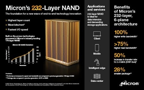
Micron Know-how has introduced the discharge of a high-density NAND with 232-layers. The NAND provides a quick NAND I/O velocity of two.4GB/s .The upper variety of layers allows the storage gadget to supply greater vitality effectivity and the trade’s highest areal density and delivers as much as 100% greater write bandwidth and greater than 75% greater learn bandwidth per die than the prior technology. The storage gadget options highest variety of aircraft per die of any TLC flash3 and options unbiased learn functionality in every aircraft. Moreover, Micron’s 232-layer NAND is the primary in manufacturing to allow NV-LPDDR4, thus making it appropriate to be used in software within the knowledge heart and on the clever edge nodes.
“Micron’s 232-layer NAND is a watershed second for storage innovation as first proof of the potential to scale 3D NAND to greater than 200 layers in manufacturing,” mentioned Scott DeBoer, govt vp of expertise and merchandise at Micron. “This groundbreaking expertise required in depth innovation, together with superior course of capabilities to create excessive side ratio constructions, novel supplies developments and modern design enhancements that construct on our market-leading 176-layer NAND expertise.”
In as we speak’s knowledge pushed world, the necessity for greater density storage gadgets is the necessity of the hour and to fulfill the rising demand, Micron Applied sciences have launched the 232-layer NAND. As well as, 232-layer NAND introduces the world’s first six-plane TLC manufacturing NAND.3 It has essentially the most planes per die of any TLC flash3 and options unbiased learn functionality in every aircraft. The mixture of excessive I/O velocity, learn and write latency, and Micron’s six-plane structure gives best-in-class knowledge transfers in lots of configurations. This construction ensures fewer collisions between write and browse instructions and drives system-level quality-of-service enhancements.
In response to the corporate, the upper variety of layers reduces the scale thus providing prospects greater flexibility of their designs whereas enabling the very best TLC density per sq. millimeter ever produced (at 14.6 Gb/mm2). The NAND is shipped in a compact 11.5mm x 13.5mm bundle, which is 28% smaller bundle measurement than earlier Micron generations.The interface can be backward appropriate to assist legacy controllers and programs. Micron’s 232-layer NAND expertise can assist superior options and real-time providers required in knowledge heart and automotive functions, in addition to responsive, immersive experiences on cellular gadgets, client electronics and PCs, and so on.
“Micron has sustained expertise management with successive first-to-market developments in NAND layer rely that allow advantages like longer battery life and extra compact storage for cellular gadgets, higher efficiency in cloud computing, and quicker coaching of AI fashions,” mentioned Sumit Sadana, chief enterprise officer at Micron. “Our 232-layer NAND is the brand new basis and customary for end-to-end storage innovation underpinning digital transformation throughout industries.”
