A semiconductor sits on the coronary heart of any digital gadget. Over the previous couple of years this trade has witnessed a increase that’s revolutionary in some ways because of the digitalisation of assorted electronics prospects together with the developments that one couldn’t have anticipated a decade in the past. Learn on to study extra about the identical
Digitalisation is the illustration of the elemental modifications within the enterprise panorama. It contains the facets of placing more and more sensible methods in place, that are able to being reconfigured on the fly and delivering new and unprecedented consumer expertise, and the way firms are digitalising their entire enterprise operations.
More and more, firms are shifting extra of their enterprise cloth onto a semiconductor framework, which is enabling them to maneuver from an on-site premise work atmosphere to distribute the work across the globe. Should you go look out out there at present, you will note a few of the following traits settling in.
Growing semiconductors content material
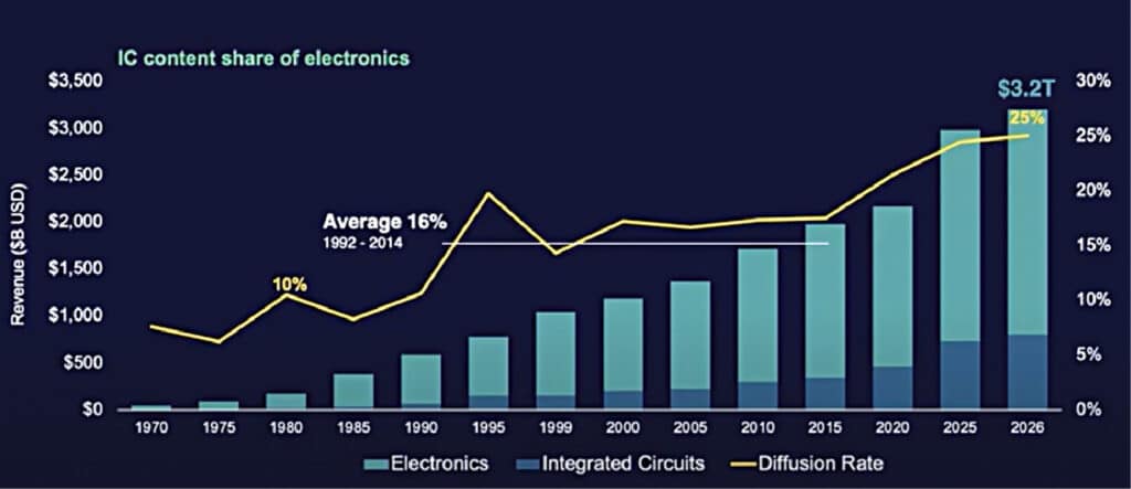
We will see within the chart in Fig. 1 that the semiconductors content material in electronics is growing steadily. Traditionally, throughout the mid-90’s this progress was at a reasonably fixed degree of about 16% of the general electronics. Contemplating the speed at which we’re placing out new sensible methods with better talents, by the yr 2026 about 25% of these machines will drive off semiconductors, therefore paving alternatives for the businesses concerned on this house.
Firms turning into SoC designers and producers
More and more the methods homes have gotten IC design firms as properly. This pattern has been witnessed within the smartphone house, whether or not it’s Apple, Google, or others. Firms working on this house have more and more began designing their very own ICs. Even in communication and automotive sectors the unique gear producers are more and more turning into designers slightly than mere customers of semiconductors.
System firms rising
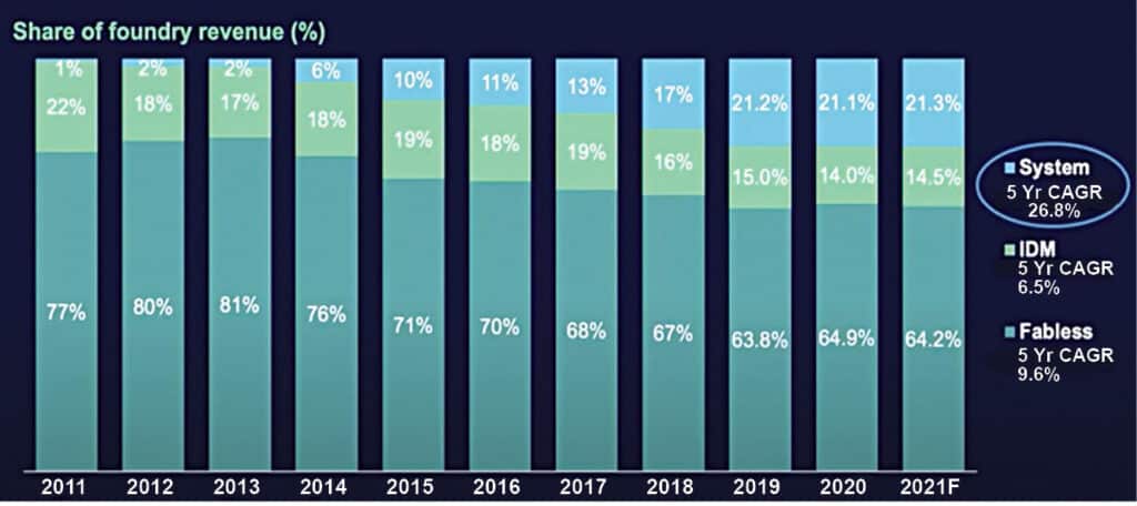
The chart in Fig. 2 reveals the share of the foundry buyer income coming from the normal built-in gadget manufacture (IDM) firms and from the brand new system firms. A decade in the past, the methods firms have been a trivial a part of the foundry income. It has now elevated and is more likely to be about 21.3% subsequent yr, which represents a compounded annual progress fee of just about 27%. Numerous that has been within the areas equivalent to Apple’s iPhone however this pattern is turning into widespread as these methods firms take increasingly management over the structure to ship a greater expertise for his or her prospects.
The 4 traits driving the digitisation methods for these firms are sensors, edge computing, 5G/wi-fi communications, and cloud/information centres. Sensors present the flexibility to digitalise the pure world and convey that right into a compute infrastructure for brand new forms of purposes. Edge computing allows integration of units into smaller footprints whereas permitting software of issues like machine studying and synthetic intelligence inside these chips. 5G offers an infrastructure that permits pulling these units collectively. Cloud and information centres permit taking this remaining set of knowledge and ship the tip purposes to the purchasers.
The chart in Fig. 3 compares the variety of sensors linked to the web in 2015 versus the quantity possible in 2025. As you’ll be able to see, in 2015 there have been about 1.6 billion sensors and by 2025 their quantity is projected to be nearly 30 billion.
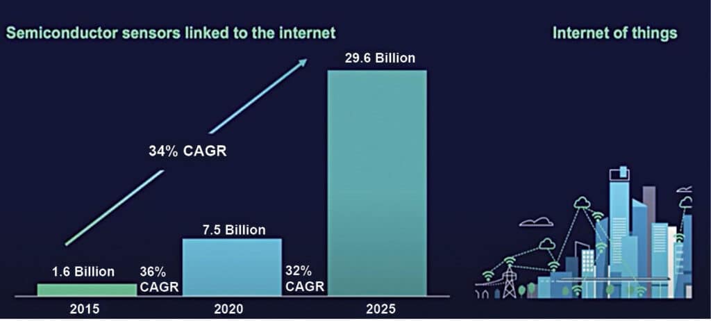
Fig. 4 reveals a robust progress alternative for 5G, which is anticipated to develop at about an 18% fee over the following few years. It additionally reveals that shopper/compute, automotive, industrial, and infrastructure/different wi-fi purposes are going to be a good bigger driver of this chance as folks begin connecting these sensors and transfer that information into the info centres.

The chart in Fig. 5 reveals a big improve in progress and alternatives in information centres themselves. It reveals a robust restoration from the dip in 2019 as a consequence of transfer to a virtualised work atmosphere due to the pandemic. For the following 5 to 6 years the rise is probably going on the fee of 11% CAGR in that giant market, driving in the direction of a 14% CAGR in later a part of the last decade.
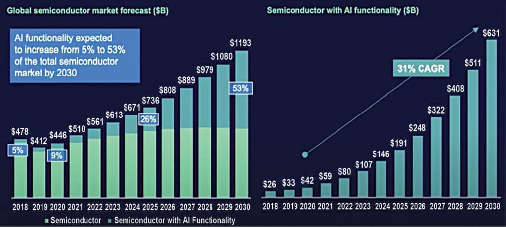
Semiconductor market progress
The chart in Fig. 5 reveals semiconductor progress shifting ahead. The chart on the left reveals predictions that appear to be lining up today for a trillion greenback semiconductor market across the yr 2030. It may be seen that there’s important distinction between baseline semiconductors and the semiconductors which have AI performance.
At current, about 10% of the chips being produced have some type of AI in them. Notable examples are cellphone software processors which have AI engines to do issues like facial recognition. About half of the market will likely be represented by chips with AI by 2030.
Explosion in world funding
The very first thing to take a look at is enterprise capital (VC) investments (see Fig. 6). Earlier than the dot-com crash, the VC investments have been about 2.5 billion {dollars}, which dropped by about 40% after the crash to about 1.7 billion {dollars} for a couple of years. In 2009, the good recession dropped that down additional to underneath 1 billion {dollars} a yr, which have been being spent on semiconductor content material. It continued to fall till 2015, when it will definitely dropped to half a billion {dollars}. Thereafter, the investments picked up sharply and in 2021 we had nearly 10 billion {dollars} funding flowing into startup firms within the semiconductor house.
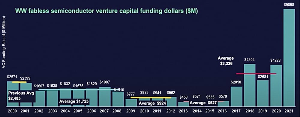
Beforehand, the vast majority of the spending was being performed in america (US) alone however now this pattern has unfold globally. China, with its well-known effort to turn into an vital supplier within the semiconductor house, has led with nearly 6.5 billion {dollars} of spending. However even the remainder of the world, outdoors of the US and China, has made about 1.6 billion {dollars} of funding into these semiconductor firms. This pattern is anticipated to extend additional as increasingly nations are realising the strategic significance of semiconductors for enabling their total financial progress.
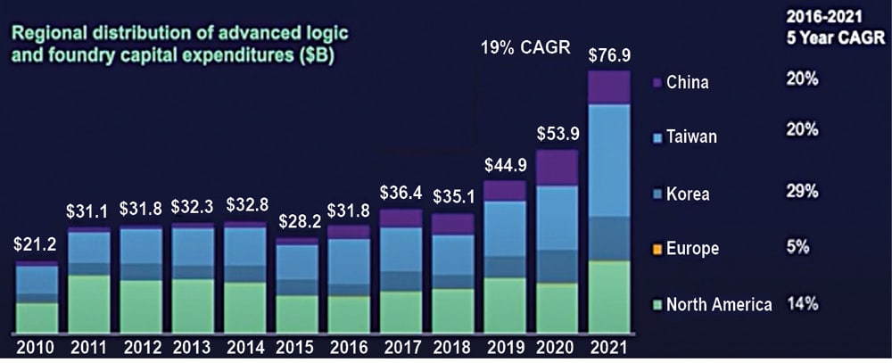
Superior logic and foundry capital investments
The chart in Fig. 7 reveals the distribution of superior logic and foundry capital expenditure. It may be seen that was a comparatively flat spending till about 2018. It began growing from the yr 2019 and reached near 80 billion {dollars} in 2021. Taiwan Semiconductor Manufacturing Firm (TSMC) has already acknowledged that they are going to spend roughly 40 billion {dollars} on enabling new foundry capability subsequent yr. So, we will anticipate to see a big improve on this quantity sooner or later.
Announcement by the Indian authorities
The federal government of India introduced roughly 10 billion {dollars} of incentives for the electronics and semiconductor trade on twenty first December final yr, which was notably encouraging for the trade. There are schemes for placing semiconductor fabs in place, schemes for placing compound semiconductor fabs, schemes for lower-end fabs in addition to meeting and check, and, lastly, schemes to work in the direction of growing design capability inside the nation.
EDA for design exercise
Within the subject of digital design automation (EDA), there’s an encouraging pattern for India. Within the final ten years worldwide, the spending on EDA has been growing at about 9%. In India it has elevated at 12% CAGR. This means that design exercise for the worldwide semiconductor trade, which has been performed largely inside India, additionally offers a very good platform on which the longer term semiconductors may be constructed.
Semiconductors have gotten a essential a part of implementing not simply near-normal electronics but in addition the businesses’ infrastructure and the way they current themselves to the world. The three pillars for enabling digitalisation for outsized progress are:
Expertise scaling. One of many basic advantages of individuals implementing this digitalisation is the truth that we will proceed with Moore’s Legislation, scale expertise, and ship extra performance on the similar value over time, which allows them to remodel themselves and have a really constructive future.
Moore’s Legislation additionally has a darkish facet. Twice as many transistors may be produced each two years which can, in flip, require twice as many transistors for use as properly. Therefore, we have to put new methodologies in place that allow us to take action.
System scaling. The appliance must get validated throughout the semiconductors earlier than these are produced to make sure that total the appliance can match inside the parameters it has. Additionally, it wants to supply the consumer expertise it’s anticipated to ship in an atmosphere the place there’s a sensor driving an edge pc that might work by 5G to the info centre.
Enabling expertise scaling
The chart in Fig. 9 for Apple’s domain-specific processor analysis reveals an eight-year time horizon, which is equal to 4 Moore’s Legislation cycles. It reveals that within the yr 2013, the A7 processor had roughly a billion transistors whereas in 2021 the A15 had roughly 15 billion transistors. It’s nearly precisely on the schedule that you’d anticipate from Moore’s Legislation.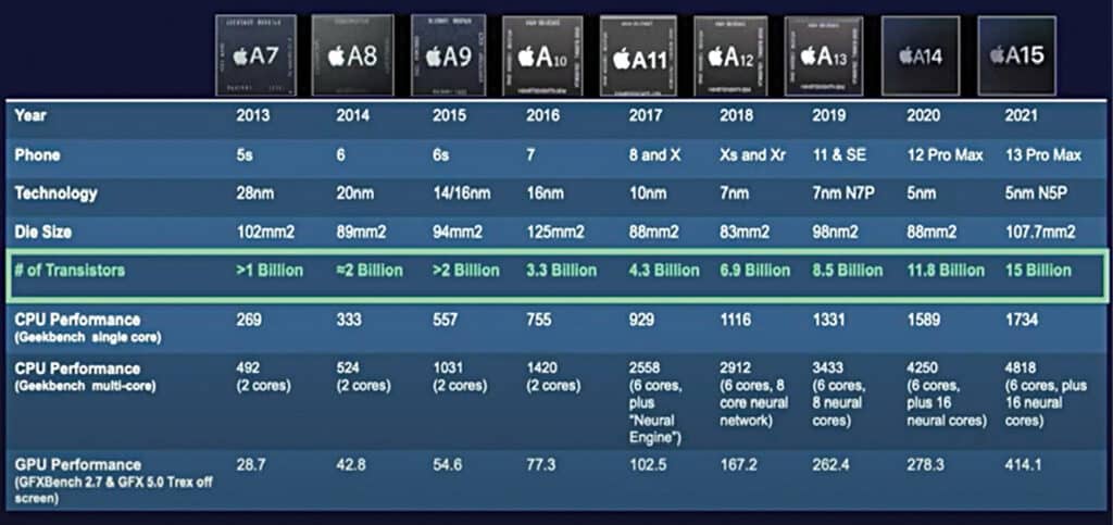
These chips carry out effectively as properly. The A7’s Geekbench single central processing unit (CPU) rating is 269 whereas for the A15 the rating stands at 1734. This improve in rating is mapped towards multi-core efficiency in addition to the graphical processing unit (GPU) efficiency.
Value scaling with design scaling
If we have been to estimate the quantity of tape outs that happen per yr and do any form of matrix multiplication of tape outs per node towards this, we are going to shortly run out of cash within the trade. We as an organization are presently doing a seven manometer (7nm) chip. The pattern line is mapped properly whether or not the numbers are precisely appropriate for any explicit chip or not.
It turns into more and more dearer to do design as we transfer down these expertise nodes. The design value doesn’t double, so the design value per transistor continues to be cheaper.
The historical past of the EDA trade has been about growing layers of abstraction. Again within the eighties, an amazing quantity of labor was performed on the transistor and SPICE (a general-purpose, open supply analogue digital circuit simulator software program utilized in IC and board-level design to test the integrity of circuit designs and to foretell circuit behaviour) degree. Within the late eighties and early nineties, the transition to RTL occurred. The transition to RTL allows us to design extra shortly.
Understanding PAVE360
Siemens launched a easy however revolutionary pre-silicon autonomous validation program, PAVE30, in Could 2019 to speed up the event of autonomous car platforms. It offers an atmosphere for multi-supplier collaboration throughout the automotive ecosystem for the event of automotive chips.
PAVE360 additionally extends digital twin simulation past processors to incorporate automotive {hardware} and software program sub-systems, full car fashions, fusion of sensor information, visitors flows, and the simulation of sensible cities by which self-driving vehicles will in the end journey.
Now we have a sensing atmosphere the place we will mannequin situations of actual world information to the place you’ll be able to put visitors lights, visitors lanes, pedestrians, and different autos, all in place that lets you run these numerous situations after which produce sensor information that may be virtualised and fed into the compute and evaluation operate.
This text relies on a tech speak at VLSI 2022 by Joe Sawicki, Government Vice President, Siemens Digital Industries Software program. It has been transcribed and curated by Laveesh Kocher, an EFY tech fanatic with a knack for open supply exploration and analysis.
Joe Sawicki is Government Vice President at Siemens Digital Industries Software program
